Co-designing the next-generation sensor for high-power automotive
Enhancing Driving Range with Advanced Current Sensor Technology
Designers and manufacturers in the electronics sector are working hard to develop solutions that will satisfy the demands of the rapidly expanding electric vehicle (EV) industry. Many companies in the sector are looking to create components or systems that will take EVs to the next level and bring the market to a higher level of maturity. The aim is to increase the driving range of EVs, adding value to Tier 1 users as well as OEMs and consumers.
This article looks at how two companies – LEM and Semikron Danfoss – have worked together to achieve those goals. In particular, it focuses on the innovation behind the development of a fully integrated LEM Nano current sensor for Semikron Danfoss’ Direct Cooled Molded (DCMTM) half-bridge power module platform.
Maximizing Power Density in EVs with Integrated SiC-MOSFET Power Modules and Current Sensors
It is widely understood that there are two key ways to achieve high power density in battery-powered traction motor drives and on/off-board chargers in EVs. One is through seamless and efficient integration while the other is to use the smallest possible power modules and current sensors (otherwise known as minimal footprint or small form factor sensors).
Through a combination of increased power density and efficiency, SiC-MOSFET power modules have made it possible to reduce size and increase the driving range. For some time, LEM and Semikron Danfoss had been working closely together to develop a technological innovation specifically targeted at electric drive trains.
Semikron Danfoss wanted to offer its customers a power module that completely integrated the sensing function while minimizing the component’s footprint. This would simplify assembly and keep costs down. Although a solution was developed that combined significant footprint reduction with a higher level of integration, an all-in-one package was the preferred option. Designers came up with a concept that would embed LEM’s current sensor into the DCMTM platform.
The 1200V class DCMTM1000X family makes use of the latest generation of 750V and 1200V SiC-MOSFETs (as well as Si-IGBTs). This means the platform can allow DC link voltage up to 1000V, satisfying the IEC 60664-1 insulation coordination standard. The module’s current capability can be scaled up to 800 Arms due to the amount of semiconductor area used.
Revolutionizing EV Traction Inverters: Introducing Compact, High-Performance Nano Current Sensor
Not only did the two companies develop a completely new assembly concept but they also created a core-based current sensor that is 60% smaller than any other core-based current sensor on the market. Also offering high bandwidth and superior immunity against cross talk, the concept can be extended to any power module, busbar or common conductor to measure currents in a fully integrated manner.
However, the new Nano current sensor is especially suitable for use with EV traction inverters that use the DCMTM platform. It is also compatible with other Semikron Danfoss power module platforms. As well as offering a high level of integration, the concept is easy to assemble and can meet all isolation requirements for 800V battery systems.
Other features of the new sensor include its ability to provide reliable performance in a wide range of challenging environments, including protection against humidity and vibrations. In particular, the device provides stability in high temperatures as well as substantially high levels of mechanical robustness.
The DCMTM1000X is a transfer molded power module with power and signal leads coming out from the side of the housing. This provides some empty space between the top side of the package and the gate driver board. The innovative idea behind the Nano concept has been the design of a core-based current sensor that can fit into this unused space. Figure 1 shows an exploded view of the assembly.
The Nano sensor delivers high degrees of accuracy, excellent immunity against external fields, high bandwidth, and a high signal-to-noise ratio (SNR) that most core-based current sensors provide. In addition, because the footprint of the current sensor is within the power module’s space claim, it does not require any extra space in the inverter.
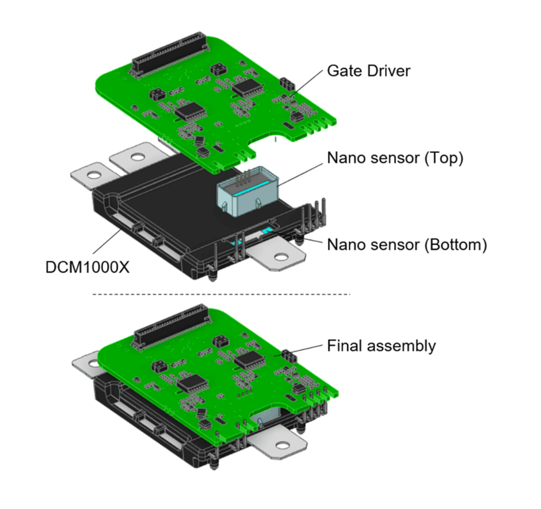
Figure 1: LEM Nano sensor integration on the DCMTM1000X
At the same time, there is no need for other components to be installed in order to fix the sensor mechanically and connect it electrically to the driver board. All of these features mean that the Nano sensor delivers the highest level of integration of any other core-based current sensor. This not only simplifies the process of vertical integration but also cuts manufacturing costs and extends the lifetime of the product.
Advanced Magnetic Core Design Enhances Accuracy and Performance of Nano Current Sensors in EV Traction Inverters
LEM designed a magnetic core surrounding the busbar with a dual air gap and a high reluctance path, tackling core saturation at higher currents and cutting flux density in the core. The company’s designers created a solution that featured two straight ferromagnetic bars – one placed on top of the AC busbar and the other underneath. Hall-plate sensing elements were positioned in the two air gaps.
LEM found that the over-mold process could be critical to the performance of the sensor. This was because it had the potential to introduce stress to the structure of the core, reduce its saturation level and increase its magnetic offset. All of these could affect overall accuracy.
With space restrictions making it impossible to oversize the core, samples over-molded at Danfoss and calibrated at LEM were checked during the assembly process. The aim was to confirm how the new concept would perform in its final configuration, including testing accuracy over a range of currents and temperatures. The over-mold process was found to have made minimal difference to the sensor’s performance, with a global offset error (magnetic + electric) below +/-5A and a sensitivity error below 3% (figure 2). Likewise, bandwidth (figure 3), step response (figure 4a and 4b) and short circuit test (figure 5) on the fully over-molded samples confirmed a response time below 3μs.
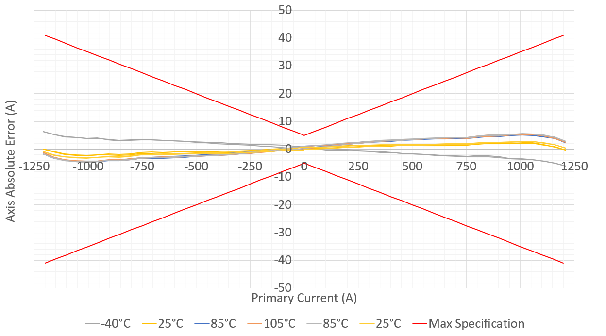
Figure 2: Global accuracy of fully over-molded sample
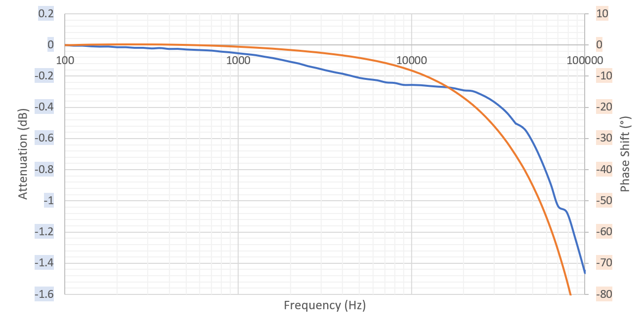
Figure 3: Bandwidth of fully over-molded sample
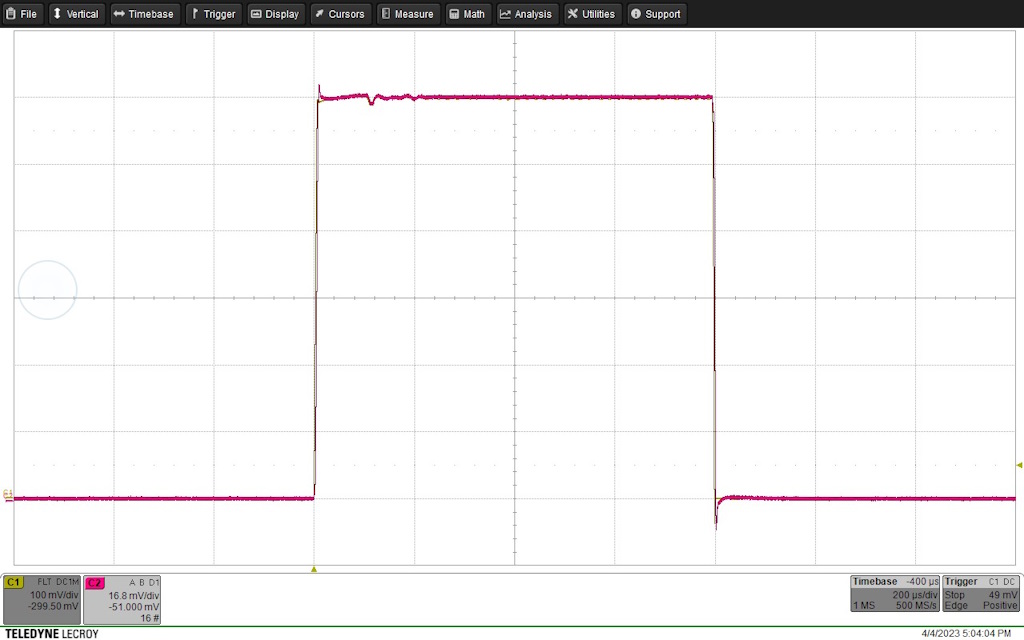
Figure 4a: Step Response of fully over-molded sample (100A/Div & 200µs/Div)
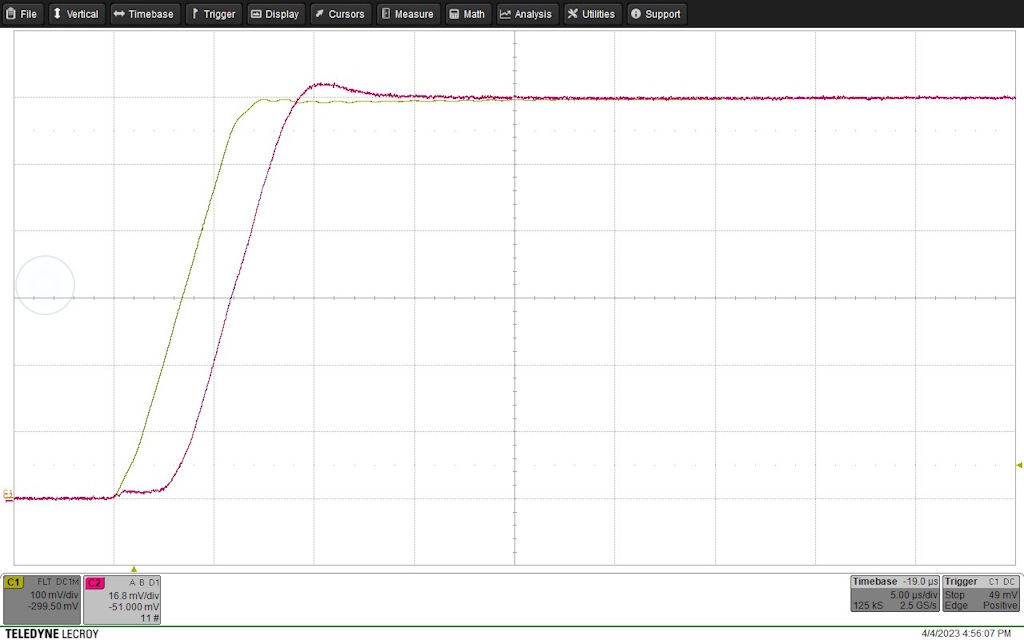
Figure 4b: Step Response of fully over-molded sample (100A/Div & 5µs/Div)
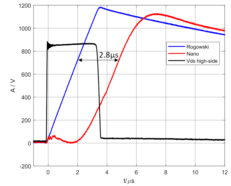
Figure 5: Results of short circuit tests on fully over-molded samples
To test the AC system level under a real inverter operation, the A-sample prototype, which has the newest generation of SiC-MOSFET, has been used as one phase of a three-phase setup that allows fast switching transients to verify the robustness of the LEM nano sensor to high dV/dt.
The following electrical parameters have been applied for the DoE (Design of Experiment): fsw=10kHz, fundamental =50Hz, PF=1, I=650Arms. The inlet water/glycol mixture temperature was maintained around 30°C and 8lt/min flow rate. A Fluxgate current sensor has been used as a performance reference. Fig.5 shows the test results with a sinusoidal modulated current.
The results obtained are in agreement with the simulation and calibration work, showing consistent results across the different current levels tested up to 650Arms.
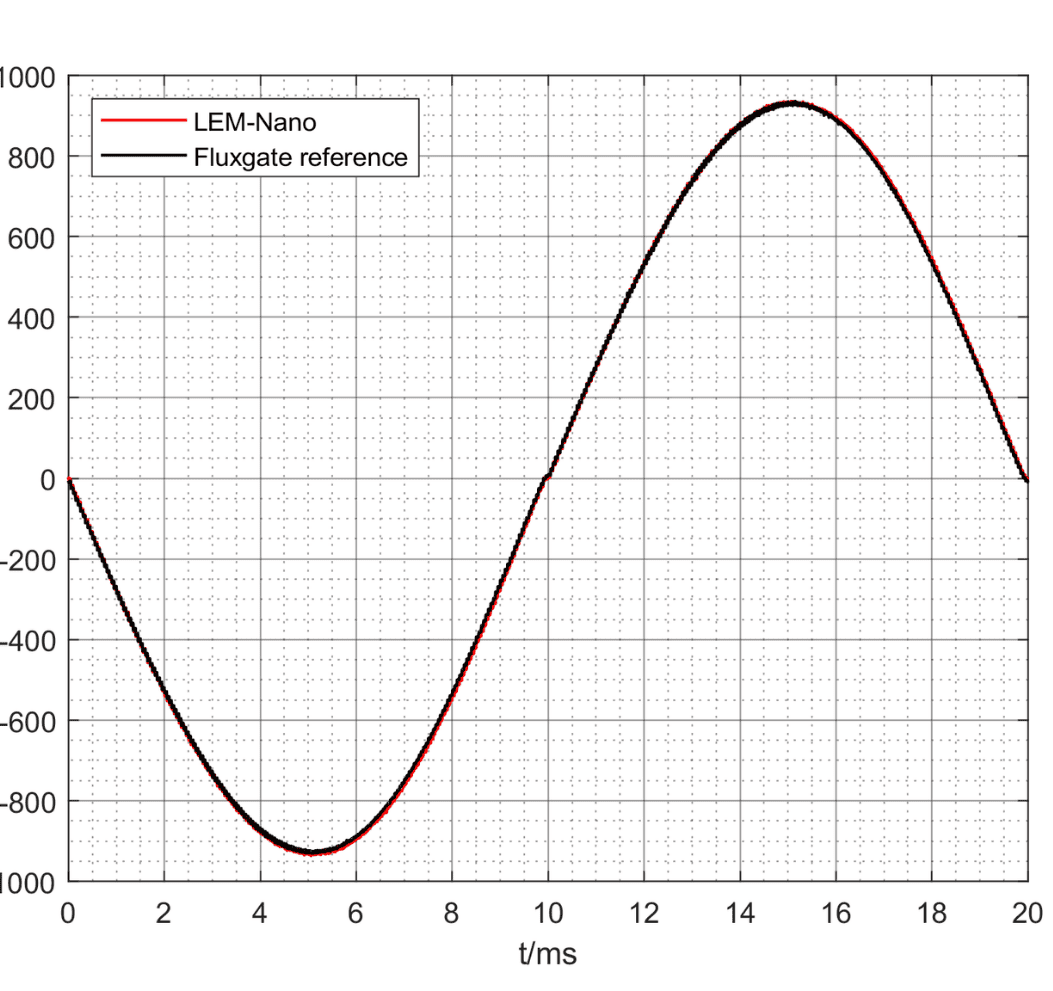
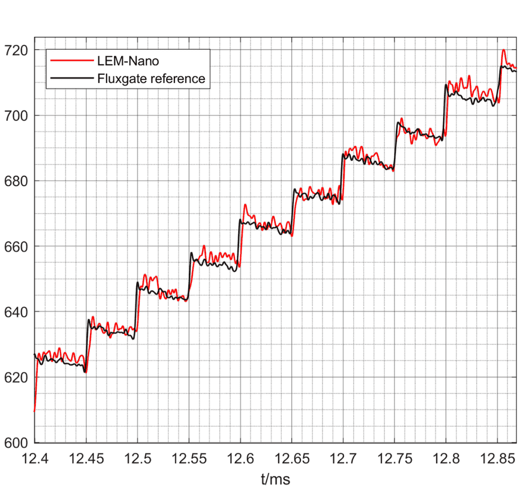
Figure 6: Test results, comparing Nano sensor with Fluxgate reference.
Traditional transfer molding processes not only don’t allow interconnection from the top, they also require high temperature curing steps of the mold compound. For these reasons, the sensor has been designed to be split. The bottom side magnetic core sits in the power module and the top side magnetic core (with its sensing elements), sits outside the power module. The final layout (figure 7) is a sandwich structure between the power module, the sensing elements, and the gate driver board. There is also a direct interconnection between the sensing element and the gate driver board.
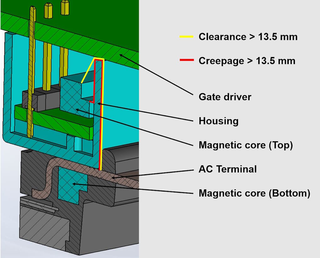
Figure 7: Cross section of the final assembly
With the interconnection of the sensor from the top of the package, it is possible to achieve a design with enough clearance and creepage distances between terminals external to the package: this means that high voltage isolation requirements can be met as well as simplifying gate driver board layout.
Internal to the package, the over-molded magnetic core is connected to the same potential as the phase terminal. A small reduction of the busbar cross section has been done to minimize the width of the magnetic core and to maximize the isolation distance between the core and the adjacent leads. This restriction doesn’t affect the mechanical stability of the busbar or create any thermal issues because it is located on a portion of the busbar that is over-molded and very close to the water-cooled substrate.
Fabio Carastro, Senior Electrical Engineer at Semikron Danfoss, says:
“Combining the Semikron Danfoss DCMTM power module, SiC-MOSFETs chips, and LEM's fully integrated sensor will truly take automotive inverters to the next level of integration and power density.”
Damien Coutellier, LEM’s senior electronics engineer and Nano project manager, adds:
“This project was a significant challenge, and its success lies in the perfect partnership with Semikron Danfoss.”